From the mid-1980s on, single electronics was established as a new branch of solid state electronics by increased research into the so-called Coulomb effects in arrays of ultrasmall tunnel elements.
46 Predictions of the correlated transfer of single electrons were proven to be true, especially on twin contacts. Structures generated by means of electron lithography were used for this at an early stage.
47 Preparation of small metallic tunnel elements was successful (in sub-micrometer dimensions), which allow the demonstration of incremental charging effects when suppressing the thermal noise and the fluctuations of quantums.
The incentive to enter this interesting field of work came from Wolfram Krech who repeatedly worked in the cryoelectronic laboratory of the State University in Moscow (K.K. Likharev, L.S. Kuzmin). At first, comprehensive theoretical studies were put into practice in the former department of Detector Physics which related to the central idea of the Coulomb blockade on twin contacts with an island electrode. The latter can be observed when two basic requirements are fulfilled:
After the transition of a single electron, the charge exchange energy of the island must be far above the level of thermal fluctuations. This requires tunnel capacities on the scale of
Femtofarad (fF) at temperatures in the range of mK.
The tunnel resistances must be greater than the so-called resistance quantum unit
h/e
2 (approx. 25.8 KΩ). This requirement conveys the negligibility of quantum fluctuations of the electrons that break the barrier (quasi-insulated island electrode).
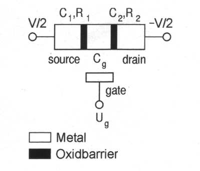 figure 18: scheme of a double contact with gate (single electron transistor)
The Coulomb blockade itself results in a threshold voltage on the twin contact which is necessary for a beginning current. This effect can be controlled by means of an additional gate electrode: the so-called single-electron-transistor (SET), figure 18, is produced from this.
As viewed from the early 1990s, specific experiments could only be conducted by the help of metallic tunnel arrays which had been manufactured by using methods of electron beam lithography. In this respect, the "angular vaporization from two angles with a suspending mask"
48 had already been distributed widely. It was applied by various groups in Europe (Göteburg, Moskau, Saclay, Delft) as well as in the USA. Working temperatures, which were conditioned by the lateral dimensions of functional components, were above 100 nm and, in general, below 50 mK. Virtually, aluminum was constantly used as a standard material. Attempts to expand shadow vaporization to niobium with the help of heat-resistant masks were absolute exceptions. In addition, sputtering methods to the deposition of thin films and the use of suspending masks cannot be applied here. Therefore, alternatives to angular vaporization were of common interest as well as of interest to us. Klaus Blüthner developed the conception of a decisive expansion of material selection by gaining access to sputtering techniques (especially the inclusion of high melting point metals) and of an increase in reproducibility and integration ability of functional components by making use of lift-off processes.
Transport of single electrons in arrays of ultrasmall tunnel contacts was experimentally and intensively explored within the scope of a research association (which was promoted by the German Federal Ministry of Education, Science, Research and Technology) at the Institute of Solid State Physics of FSU, Jena from 1994 to 2000. At the beginning of works, there were well-balanced experiences in the deposition of thin films and structuring, and the provision of cryogenic media was ensured by the own condenser. The cryoelectronic measuring equipment and its core piece, a He
3/He
4 hybrid cryostat (Kelvinox 400, company Oxford Instruments), worked without any problems. Co-operation with the Institute of Applied Physics (IAP) of FSU in Jena, which brought both the equipment for structuring of thin films and the employees for the preparation of nanometric single electronic devices as an agent of the former company LS Leica GmbH, was most significant in working together with associate partners. There was also an active exchange of experiences with the Physikalisch-Technische Bundesanstalt (PTB) in Braunschweig, the Institute for General and Theoretical Electrical Engineering of the University of Technology in Ilmenau and the IPHT e.V. in Jena as well as the University of Bayreuth (nonprofit support in terms of low temperature technics).
It was our intention to overcome all the disadvantages of the technics of cast shadows, which is described above, and it first led us to the so-called self-aligned in-line (SAIL) conception of the preparation of ultrasmall metallic edge tunnels
49 (figure 19).
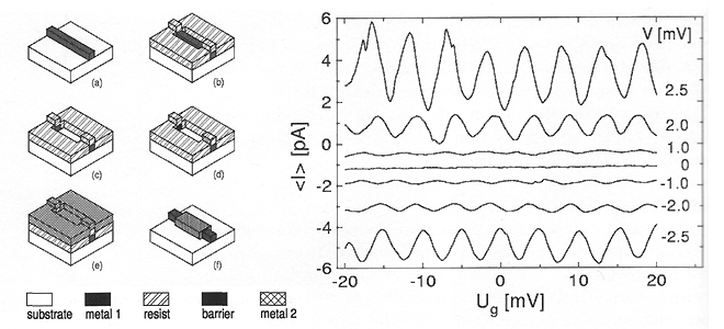 figure 19: Left: diagram of preparation method SAIL; right: modulation characteristic of a superconducting Nb/AlOx/Nb-SET (T=300mK)
By comparison with the shadow vaporization, the following advantages of the SAIL technology can be found: The way of the deposition process is freely selectable, both vaporizing and sputtering are possible. The latter is more suitable for high melting point materials; sensitive suspending masks are not needed for this. Contact masks are heat-resistant and can be used as lift masks at the same time. Lateral shadows are not visible as opposed to the two-angle vaporization.
The SAIL preparation was needed to the fabrication of different single-charge transistors. In the mid-1990s, the prototype of the Nb/AlO
x/Nb based transistor (All the electrodes are made of niobium.) could already be presented internationally for the first time.
50 Its typical characteristics are illustrated in figure 19b (data: gate capacity C
Σ ~ 3 × 10
-17 F, island capacity C
Σ ~ 3 × 10
-16 F, superconducting energy gap 2Δ/e ~ 1,0 mV).
Unfortunately, the single-electron transistors that had been fabricated according to the practiced SAIL version had – which became more and more clearly in the continuous process – a tendency to redeposition of the sputtered material of metal edges that were vertically positioned to the substrate. That sediment naturally results from openings in the resist with high aspect ratio. The diffusion of tunnel resistances on different scales involved made Thomas Wagner, Detlef Born und Uwe Hübner conceptualize a modified production technique which maintains the advantages of the SAIL method, viz. the electron beam lithography in connection with the deposition of thin films by sputtering.
Now, the structures are transferred to the resist by direct writing with the electron beam.
51 The sequence of the most important steps is delineated in figure 20a:
(1) Fabrication of the feed line electrodes and the gate
· Resist mask (PMMA stands for polymethylmethacrylate which is also known under the name of acrylic glass)
· Electron beam exposure
· Sputtering of the electrode material
· Lift-off process
(2) Fabrication of the island electrode and the tunnel barriers
· Resist mask for generating the island
· Exposure; exposed areas of the feed line electrodes make up the contact surfaces
· Fabrication of barriers
· Sputtering of the island material
· Lift-off process
The line widths of the metal tapes are less than 100 nm, the tunnel capacities are below 0,5 fF. A double undercut, which prevents disturbing redepositions and guarantees a perfect overlap of subsequent deposited thin films (figure 20), was made by a special 4-layered resist system. This technique was successfully applied to the fabrication of SETs based on the metals of aluminum and niobium.
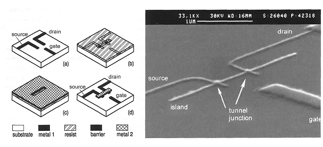 figure 20: Left: diagram of direct writing with an electron beam; right: SEM micrograph of an Al/AlOx/Al-SET
In general, the options explained can be used for the fabrication of metallic nanostructures. The co-operations with the IPHT, IAP and IFK helped develop superconducting qubits in Jena about 1999/2000 which would be possible components of future quantum computers. The so-called charging qubits of the interferometer type have been introduced at the IFK lately.
52 The following chapter deals with analog works on flux qubits.
literature
46. Averin, D. V. / Likharev, K. K.: Coulomb Blockade of Single-Electron Tunneling and Coherent Oscillations in Small Tunnel Junctions. In: J. Low Temp. Phys. 62 (1986)
47. Fulton, T. A. / Dolan, G. J.: Observation of Single-Electron Charging Effects in Small Tunnel Junctions. In: Phys. Rev. Lett. 59 (1987)
48. Niemeyer, J.: Eine einfache Methode zur Herstellung kleinster Josephson-Elemente. In: PTB-Mitteilungen. 4/74 (1974)
49. Götz. M. / Blüthner, K. / Krech, W. / Nowack, A. / Fuchs, H. - J. / Kley, E. - B. / Thieme, P. / Wagner, Th. / Eska, G. / Hecker, K. / Hegger, H.: Preparation of Self-Aligned In-Line tunnel Juncions for Applications in Single-Charge Electronics. In: J. Appl. Phys. 78 (1995)
50. Blüthner, K. / Götz, M. / Hädicke, A. / Krech, W. / Wagner, Th. / Mühlig, H. / Fuchs, H.-J. / Hübner, U. / Schelle, D. / Kley, E.-B.: Single-Electron Transistors Based on Al/AlOx/Al and Nb/AlOx/Nb Tunnel Juncions. In: IEEE Trans. Appl. Supercond. 7 (1997)
51. Born, D. / Wagner, Th. / Krech, W. / Hübner, U. / Fritzsch, L.: Fabrication of Ultrasmall Tunnel Junctions by Electron Beam Direct-Writing. In: IEEE Trans. Appl. Supercond. 11 (2001)
52. Shnyrkov, V. I. / Wagner, Th. / Born, D. / Shevchenko. S. N. / Krech, W. / Omelyanchouk, A. N. / Il'ichev, E. / Meyer, H.-G.: Multiphoton transistions between energy levels in a phase-biased Cooper-pair. In: Phys. Rev. B 73 (2006)
« back
Contact us
Supracon AG
An der Lehmgrube 11
07751 Jena
Germany
Tel.: +49-3641-2328100
Fax.: +49-3641-2328109
info(at)supracon.com
