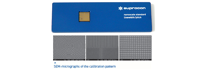
The Nanoscale Linewidth / Pitch standard contains patterns on the nanometer scale for the linewidth calibration and resolution - check of high - resolution optical microscopy techniques like deep ultraviolet microscopy (UVM) and confocal laser scanning microscopy (CLSM). It can be used for quick astigmatism testing of these instruments and also for scanning probe methods like atomic force microscopy (AFM).
The Nanoscale Linewidth / Pitch standard consists of different grating structures etched in nanocrystalline silicon on a quartz substrate.
The optical contrast of the pattern in the UV wavelength makes it suitable for transmission and reflection UV and laser scanning microscopy. The types of grating are 1-dim (for both x and y), 2-dim (cross grating) and circular.
An isolated single structure for CD determination is added on one side of the 1-dim grating.
The pitch values are 160, 200, 230, 260, 300, 400, 500, 700 nm, 1 μm and 4 μm, i.e. the structure widths are between 80 nm and 2 μm.
With the exception of the larger 4 μm-structures each grating has an area of around 10×10 μm².
| Specification | |
| Substrate | Material: quartz
chip dimension: 8×8 mm²
|
| Film | Nanocrystalline silicon
Thickness: 25 nm
|
| Chip holder | Size: 76×26×2 mm
Material: aluminium alloy, anodized
|
| Finding structures | Au
Thickness: 100 nm
|
| Types of grating | 1-dim (for both x and y)
2-dim (cross grating)
Circular grating
An isolated single structure for CD determination is added on one side of the 1-dim grating
|
| Size of grating | Normally 10×10 μm²
|
| Linewidths of the CD-structure | Nominal: 80 nm, 100 nm, 115 nm, 130 nm, 200 nm, 250 nm, 350 nm, 500 nm, 2 μm
Linewidth variation along the lines (within a central part of 6 µm): 8 nm 1σ
|
| Pitches | 160 nm, 200 nm, 230 nm, 260 nm, 300 nm, 400 nm, 500 nm, 700 nm, 1000 nm, 4 μm
Uncertainty of mean pitch: 3 nm 1σ
|
| Circularity of the circular gratings | ± 0.6 % deviation of mean pitch in x- and y-direction(± 1 nm for 160 nm grating)
|
| Traceability | CD & pitch-calibration made by the PTB Braunschweig on request |
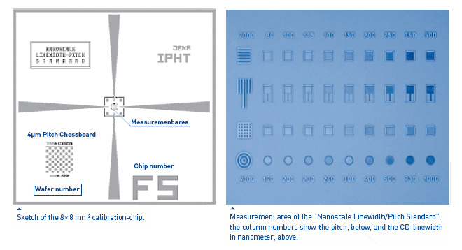
Chip and pattern description
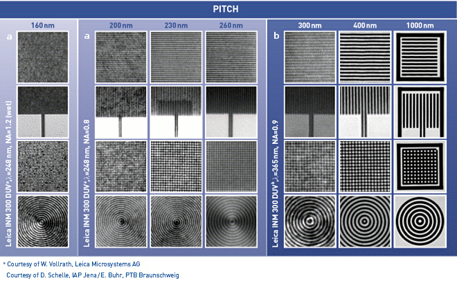
DUV-images
The picture shows DUV-images obtained from the structures of the Nanoscale Linewidth /Pitch Standard by using different kinds of optical lenses. The column numbers indicate the pitch in nanometers. Only the high resolution DUV-microscope (λ = 248 nm) using an immersions objective (NA = 1.2) is able to provide clear pictures of the 160 nm-gratings.
« back
Contact us
Supracon AG
An der Lehmgrube 11
07751 Jena
Germany
Tel.: +49-3641-2328100
Fax.: +49-3641-2328109
info(at)supracon.com